- 您现在的位置:买卖IC网 > Sheet目录239 > NZQA6V8XV5T1G (ON Semiconductor)TVS ARRAY QUAD ESD 6.8V SOT553
NZQA5V6XV5T1G Series
ELECTRICAL CHARACTERISTICS
(T A = 25 ° C unless otherwise noted)
Symbol Parameter
I PP
Maximum Reverse Peak Pulse Current
V C
Clamping Voltage @ I PP
I F
I
I R V F
V RWM
I R
Working Peak Reverse Voltage
Maximum Reverse Leakage Current @ V RWM
V C V BR V RWM
I T
V
V BR
I T
Breakdown Voltage @ I T
Test Current
Q V BR
I F
V F
Z ZT
I ZK
Z ZK
Maximum Temperature Coefficient of V BR
Forward Current
Forward Voltage @ I F
Maximum Zener Impedance @ I ZT
Reverse Current
Maximum Zener Impedance @ I ZK
I PP
Uni ? Directional
MAXIMUM RATINGS (T A = 25 ° C unless otherwise noted)
Characteristic
Peak Power Dissipation (8 X 20 m s @ T A = 25 ° C) (Note 1)
Steady State Power ? 1 Diode (Note 2)
Thermal Resistance Junction to Ambient
Above 25 ° C, Derate
Maximum Junction Temperature
Operating Junction and Storage Temperature Range
Symbol
P PK
P D
R q JA
T Jmax
T J T stg
Value
100
300
370
2.7
150
? 55 to +150
Unit
W
mW
° C/W
mW/ ° C
° C
° C
ESD Discharge
MIL STD 883C ? Method 3015 ? 6
IEC1000 ? 4 ? 2, Air Discharge
V PP
16
16
kV
IEC1000 ? 4 ? 2, Contact Discharge
9
Lead Solder Temperature (10 seconds duration)
T L
260
° C
Stresses exceeding Maximum Ratings may damage the device. Maximum Ratings are stress ratings only. Functional operation above the
Recommended Operating Conditions is not implied. Extended exposure to stresses above the Recommended Operating Conditions may affect
device reliability.
ELECTRICAL CHARACTERISTICS (T A = 25 ° C)
Device
Breakdown Voltage
V BR @ 1 mA (Volts)
Leakage Current
I RM @ V RM
V C Max @ I PP
Typ Capacitance
@ 0 V Bias
(Note 3)
Max
V F @ I F =
200 mA
Device
NZQA5V6XV5T1G
NZQA6V2XV5T1G
NZQA6V8XV5T1G
Marking
56
62
68
Min
5.32
5.89
6.46
Nom
5.6
6.2
6.8
Max
5.88
6.51
7.14
V RWM
3.0
4.0
4.3
I RWM ( m A)
1.0
0.5
0.1
V C (V)
10.5
11.5
12.5
I PP (A)
10
9.0
8.0
(pF)
90
80
70
(V)
1.3
1.3
1.3
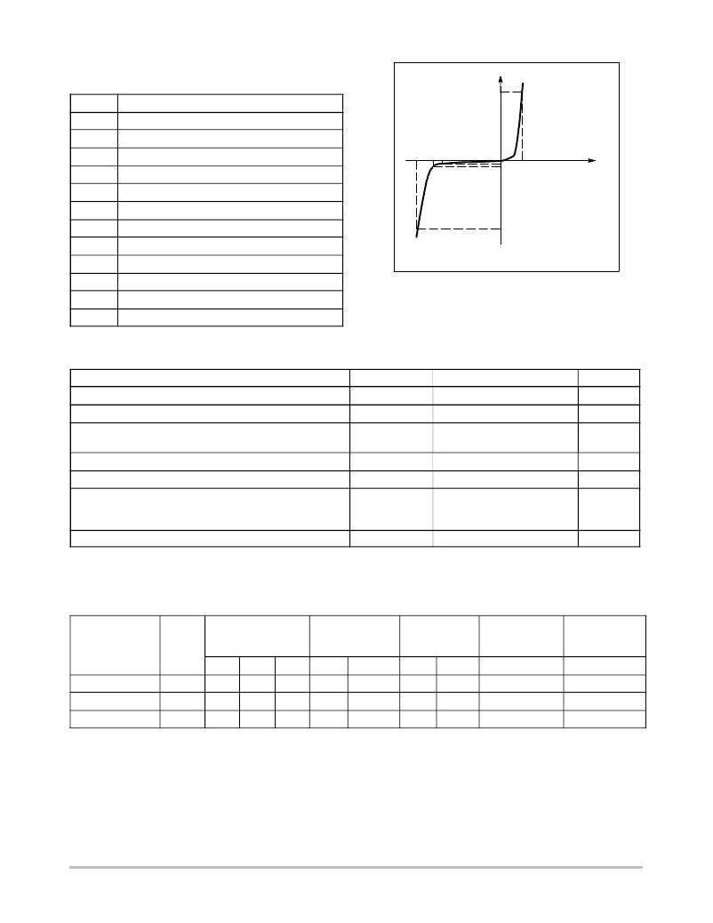
1. Non ? repetitive current per Figure 1.
2. Only 1 diode under power. For all 4 diodes under power, P D will be 25%. Mounted on FR ? 4 board with min pad.
3. Capacitance of one diode at f = 1 MHz, V R = 0 V, T A = 25 ° C
http://onsemi.com
2
发布紧急采购,3分钟左右您将得到回复。
相关PDF资料
OMNI1000ISO
UPS 1000VA 700W 6OUT USB TOWER
OMNI1500XLNAFTA
UPS 1500VA 940W 8OUT TOWER
OMNI300NAFTA
UPS 300VA 180W 3OUT TOWER
OMNI500ISO
UPS 500VA 300W 3OUT USB TOWER
OMNI650LCD
UPS 650VA 8OUT LCD DISP USB
OMNI750ISO
UPS 750VA 500W 6OUT USB TOWER
OMNI900LCD
UPS 900VA 8OUT LCD DISP USB
OMNISMART1050
UPS 1050VA 705W 6OUT W/SOFTWARE
相关代理商/技术参数
NZQA6V8XV5T2
功能描述:TVS二极管阵列 SOT553 QUAN ZNR RoHS:否 制造商:Littelfuse 极性: 通道:4 Channels 击穿电压: 钳位电压:11.5 V 工作电压:2.5 V 峰值浪涌电流:20 A 安装风格:SMD/SMT 端接类型:SMD/SMT 系列: 最小工作温度:- 40 C 最大工作温度:+ 85 C
NZSMB15CAT3
功能描述:TVS 二极管 - 瞬态电压抑制器 ZEN SMB TVS CLP 400W SPCL RoHS:否 制造商:Vishay Semiconductors 极性:Bidirectional 工作电压: 击穿电压:58.9 V 钳位电压:77.4 V 峰值浪涌电流:38.8 A 系列: 封装 / 箱体:DO-214AB 最小工作温度:- 55 C 最大工作温度:+ 150 C
NZSMB15CAT3G
功能描述:TVS 二极管 - 瞬态电压抑制器 ZEN SMB TVS CLP 400W SPCL RoHS:否 制造商:Vishay Semiconductors 极性:Bidirectional 工作电压: 击穿电压:58.9 V 钳位电压:77.4 V 峰值浪涌电流:38.8 A 系列: 封装 / 箱体:DO-214AB 最小工作温度:- 55 C 最大工作温度:+ 150 C
NZSMB30CAT3
功能描述:TVS 二极管 - 瞬态电压抑制器 ZEN SMB TVS CLP 400W SPCL RoHS:否 制造商:Vishay Semiconductors 极性:Bidirectional 工作电压: 击穿电压:58.9 V 钳位电压:77.4 V 峰值浪涌电流:38.8 A 系列: 封装 / 箱体:DO-214AB 最小工作温度:- 55 C 最大工作温度:+ 150 C
NZSMB30CAT3G
功能描述:TVS 二极管 - 瞬态电压抑制器 ZEN SMA TVS CLP 400W SPCL RoHS:否 制造商:Vishay Semiconductors 极性:Bidirectional 工作电压: 击穿电压:58.9 V 钳位电压:77.4 V 峰值浪涌电流:38.8 A 系列: 封装 / 箱体:DO-214AB 最小工作温度:- 55 C 最大工作温度:+ 150 C
NZT44H8
功能描述:两极晶体管 - BJT NPN Power Transistor RoHS:否 制造商:STMicroelectronics 配置: 晶体管极性:PNP 集电极—基极电压 VCBO: 集电极—发射极最大电压 VCEO:- 40 V 发射极 - 基极电压 VEBO:- 6 V 集电极—射极饱和电压: 最大直流电集电极电流: 增益带宽产品fT: 直流集电极/Base Gain hfe Min:100 A 最大工作温度: 安装风格:SMD/SMT 封装 / 箱体:PowerFLAT 2 x 2
NZT45C11
制造商:FAIRCHILD 制造商全称:Fairchild Semiconductor 功能描述:PNP Current Driver Transistor
NZT45H8
功能描述:两极晶体管 - BJT PNP Power Transistor RoHS:否 制造商:STMicroelectronics 配置: 晶体管极性:PNP 集电极—基极电压 VCBO: 集电极—发射极最大电压 VCEO:- 40 V 发射极 - 基极电压 VEBO:- 6 V 集电极—射极饱和电压: 最大直流电集电极电流: 增益带宽产品fT: 直流集电极/Base Gain hfe Min:100 A 最大工作温度: 安装风格:SMD/SMT 封装 / 箱体:PowerFLAT 2 x 2
